


Flexible Devices
With excellent mechanical flexibility and ultra-thin dimensions, 2D materials can be integrated onto flexible substrates for next-generation flexible optoelectronic devices.
Transparent Electrodes
2D materials combine high optical transparency with excellent electrical conductivity, making them promising transparent electrodes for next-generation optoelectronic devices.
Photovoltaic Devices
2D materials offer excellent light absorption and carrier transport properties, enabling the development of efficient thin-film photovoltaic devices.
Photodetectors
2D materials offer high surface-to-volume ratios and tunable optoelectronic properties, enabling highly sensitive and fast-response photodetectors.
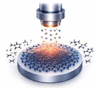
Thin-film deposition techniques, including sputtering, atomic layer deposition (ALD), and chemical vapor deposition (CVD), enable the controlled growth of large-area 2D materials with tunable thickness and layer numbers.
Seqential Growth
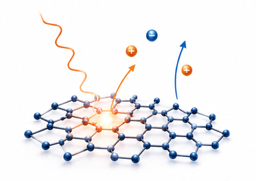
The effects of photogenerated carriers, interfacial effects, and band structures are investigated to elucidate the optoelectronic mechanisms governing 2D material devices.